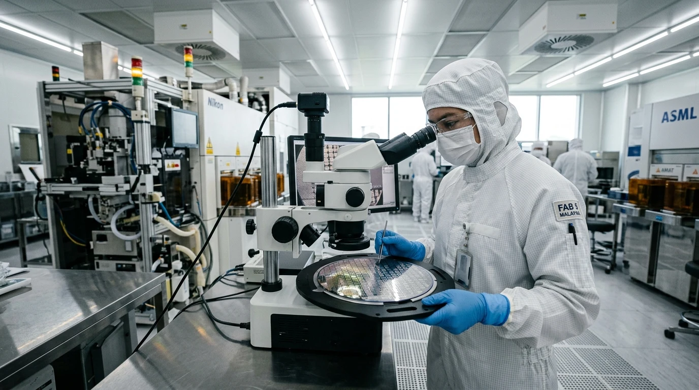
Semiconductor Wafer Dicing & Packaging Logistics in Malaysia: The Complete Industry Guide
✨ This article was AI edited. Editorial responsibility: The Future Warehouse.
Malaysia is a critical cornerstone of the global semiconductor supply chain, accounting for approximately 13% of the worldwide semiconductor packaging, assembly, and testing (OSAT) market. Within this high-technology manufacturing landscape, the wafer dicing and die preparation business in Malaysia—anchored in the industrial hubs of Penang (Bayan Lepas and Batu Kawan), Kulim Hi-Tech Park (Kedah), and Johor—plays a pivotal role in transforming fabricated silicon wafers into individualized microchips for automotive, artificial intelligence, industrial IoT, and consumer electronics worldwide.
What is Semiconductor Wafer Dicing and Die Singulation?
In semiconductor manufacturing, integrated circuits (ICs) are fabricated in hundreds or thousands of identical dies on a single round silicon wafer (typically 200mm/8-inch or 300mm/12-inch diameters). Wafer dicing (singulation) is the precision mechanical or laser process of cutting the wafer along designated “dicing streets” (scribe lines) to separate individual integrated circuit chips without damaging the delicate microscopic microcircuits.
Primary wafer dicing methodologies deployed in Malaysian OSAT facilities include:
- Mechanical Blade Dicing: High-speed diamond grit circular dicing blades rotating at 30,000 to 60,000 RPM cooled by ultra-pure deionized (DI) water jets. The standard industry approach for silicon wafers with thicknesses above 100 microns.
- Laser Ablation Dicing: Short-pulse UV or green laser beams that vaporize dicing street material with zero mechanical stress, ideal for thin wafers and ultra-narrow street geometries.
- Stealth Dicing (Internal Laser Cleaving): An infrared laser focuses inside the silicon substrate to create a localized micro-damage layer, followed by mechanical tape expansion to cleave the dies with zero surface contamination and zero kerf width loss.
- Plasma Dicing (Deep Reactive-Ion Etching / DRIE): Chemical dry etching separating thousands of dies simultaneously at the wafer level, maximizing die yields on ultra-dense wafer layouts.
Overview of the Malaysian Semiconductor Packaging Ecosystem
The Malaysian semiconductor ecosystem offers a fully integrated value chain from substrate preparation to export air logistics:
| Industrial Cluster / Region | Key Manufacturing Strengths | Major Industry Players | Logistics & Export Gateways |
|---|---|---|---|
| Penang (Silicon Island of the East) | Advanced OSAT, wafer dicing, flip-chip packaging, wafer-level chip scale packaging (WLCSP) | Inari Amertron, ASE Group, Intel, Carsem, TF AMD, Micron | Penang International Airport (PIA Cargo Hub), Butterworth Port |
| Kulim Hi-Tech Park (KHTP, Kedah) | Silicon wafer fabrication, compound semiconductors (SiC/GaN), power electronics dicing | Infineon Technologies, SilTerra, AT&S, Fuji Electric | Direct bonded road transport to Penang Air Cargo |
| Johor / Southern Corridor | EMS assembly, cleanroom packaging, precision mechanical tooling, ESD storage | V.S. Industry, ATA IMS, Jabil Johor, Western Digital | Senai International Airport, Port of Tanjung Pelepas (PTP) |
| Klang Valley / Selangor | Automotive IC packaging, leadframe manufacturing, test and tape-and-reel services | Unisem, Texas Instruments, NXP Semiconductors | Kuala Lumpur International Airport (KLIA Cargo), Port Klang |
Cleanroom Logistics, ESD Protection & Storage Protocols
Silicon dies after dicing are extraordinarily sensitive to micro-particle contamination, electrostatic discharge (ESD), mechanical vibration, and relative humidity. Warehousing and transporting diced wafers requires specialized semiconductor logistics protocols:
1. ISO Class 5 to Class 7 Cleanroom Warehousing
Dicing and pick-and-place tape-and-reel packing occur within certified cleanroom environments maintaining positive air pressure, HEPA laminar airflow filtration, and temperature controls tightly regulated at 22°C ± 1°C and 45% ± 5% relative humidity (RH).
2. Electrostatic Discharge (ESD) Mitigation
All packaging materials—including dicing rings, wafer grip tape, conductive waffle packs, gel-paks, and thermoformed embossed carrier tapes—must meet ANSI/ESD S20.20 standards with surface resistivities between 10^4 and 10^9 ohms/sq to eliminate static shock events.
3. Nitrogen Purge Cabinet Storage (Dry Box Buffers)
Bare singulated dies with exposed aluminum or copper bond pads are stored in sealed nitrogen (N2) dry storage cabinets to prevent pad oxidation prior to die-attach and wire-bonding processes.
4. Automated Optical Inspection (AOI) and Die Defect Classification
Following high-speed dicing, automated optical inspection scanners scan 100% of singulated dies under high-magnification multi-spectrum illumination. AI vision algorithms instantly identify backside chipping (kerf damage), bond pad corrosion, top passivation scratches, and silicon micro-cracks, generating electronic wafer maps that instruct robotic die-sorters to pick only grade-A certified silicon.
Establishing a Dicing or OSAT Supply Chain Business in Malaysia
Entrepreneurs and multinational technology corporations establishing wafer processing or cleanroom packaging facilities in Malaysia benefit from robust institutional support:
- MIDA Pioneer Status & Investment Tax Allowances: The Malaysian Investment Development Authority (MIDA) offers corporate income tax exemptions up to 100% for 5 to 10 years for qualifying high-tech wafer processing investments.
- Free Commercial Zones (FCZ) & Licensed Manufacturing Warehouses (LMW): Establishing operations within Free Industrial Zones (FIZs) in Penang or Kulim enables duty-free import of raw silicon wafers, diamond blades, and cleanroom consumables, as well as fast-track customs clearance for air exports.
- Access to Skilled Engineering Talent: Regional universities (Universiti Sains Malaysia, Penang Skills Development Centre) provide specialized technical curricula in semiconductor packaging and precision micro-machining.
Global Air Freight Integration for High-Value Microchips
Because semiconductor microchips exhibit high value-to-weight ratios, virtually 100% of finished diced wafers and packaged microchips are exported via air freight. Scheduled dedicated freighter flights from Penang International Airport (PIA) connect directly to tech assembly epicenters in Taipei, Seoul, Tokyo, Singapore, Munich, and Silicon Valley within 24 to 48 hours.
Related Advanced Logistics & Packaging Guides
To understand the broader spectrum of precision storage, packaging technologies, and modern automated fulfillment systems, explore our specialized guides on advanced industrial packaging methods and automated robotics in modern warehouse ecosystems.
Conclusion: The Strategic Future of Malaysian Semiconductor Dicing
As the global demand for generative AI accelerators, autonomous automotive electronics, and 5G communication infrastructure accelerates, Malaysia’s wafer dicing and advanced packaging sector continues to expand. With multi-billion dollar capital expansions in Kulim and Batu Kawan, the nation solidifies its standing as an indispensable microelectronics packaging powerhouse.
Get our latest guides, news, and insights highlighted in your Google Search & AI Overviews.


